Thermoforming for the electronics industry

  • Thermoformed packaging with conductive and dissipative ESD properties that protect sensitive electronic components.
  • Design of WIP and dunnage trays for organization, transport, and efficient assembly of parts.
  • Protection against electrostatic discharge, vibration, and contamination during production and logistics processes.
  • Customized solutions with precise dimensional control for electronic cards, semiconductors, and assemblies.
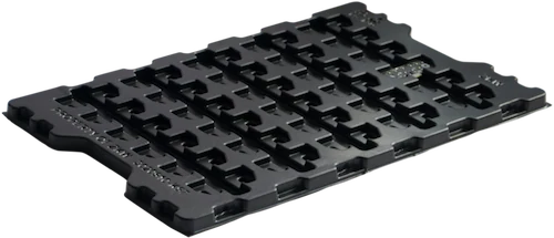
ESD WIP tray for the electronics industry

Thermoformed packaging for the electronics industry

We develop specialized thermoformed packaging for the electronics industry, designed to protect sensitive components against electrostatic discharge and mechanical damage. We manufacture trays, WIP trays, and dunnage with conductive or dissipative ESD materials that guarantee safety, order, and efficiency in manufacturing, assembly, and logistics processes for electronic products.

Electrostatic Properties

Conductive or dissipative properties that control the accumulation and discharge of static electricity, protecting sensitive components during handling, assembly, and transport.

Rigidity and Protection

High structural rigidity and mechanical resistance, providing dimensional support, impact protection, and stability during handling, stacking, and transport of electronic components.

Thermoformed packaging in the electronics industry

These thermoformed ESD trays are used for handling and protecting motherboards, assembled electronic cards (PCBAs), semiconductors, chips and integrated circuits, electronic modules and sensors, as well as connectors, SMT components, power supplies, hard drives, storage components, and electronic assemblies for industrial, automotive, and telecommunications applications.
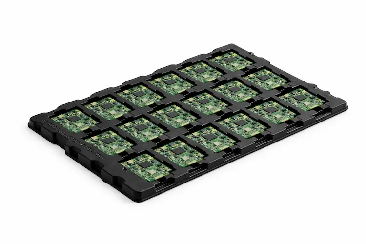
Thermoformed HIPS ESD tray for PCB boards

Motherboards

PCBs require thermoformed trays with dimensional control and ESD properties that protect their tracks and components during manufacturing, assembly, and transport.
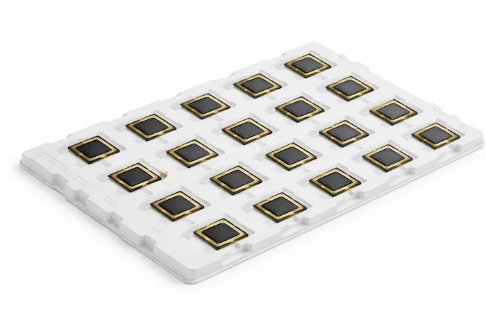
Thermoformed ESD tray for semiconductors

Semiconductors

Semiconductors need ESD thermoformed packaging that dissipates electrostatic charges and prevents electrical and mechanical damage in critical processes.
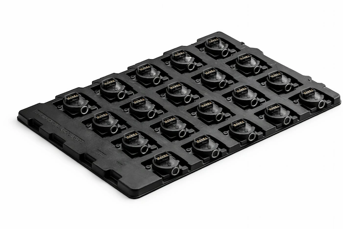
Thermoformed ESD tray for electronics packaging

Sensors

Electronic sensors use thermoformed trays that ensure physical protection, dimensional stability, and ESD control to maintain their precision and operation.

FAQ

ESD Trays: FAQs

Have another question? Write to us and our team will answer.

Request a quote →

What is the difference between a conductive and a dissipative ESD tray?

Both control static electricity. A conductive tray has very low surface resistance (below 1×10⁵ ohms) and discharges static immediately; a dissipative tray (between 1×10⁵ and 1×10¹¹ ohms) releases it gradually and in a controlled way. We choose the right one based on how sensitive your component is.

Which components do you make ESD trays for?

PCBs and PCBAs, semiconductors, chips and integrated circuits, modules and sensors, connectors, SMT components, power supplies and assemblies for industrial, automotive and telecom applications.

Do you make custom WIP trays and dunnage?

Yes. We design WIP trays and dunnage around the geometry of each part, with dimensional control for manufacturing, assembly, stacking and shipping.

Quality and food-safety certificationsWe manufacture to international standards.

ISO 9001:2015FSSC 22000SMETA

Have a thermoformed packaging project?

Tell us about your product and our engineering team will help you design the right packaging.

Request a quote →